![]()
|
|
||
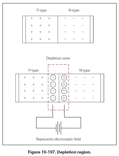
PN Junctions and the Basic Diode A single type of semiconductor material by itself is not very useful. Useful applications are developed only when a single component contains both P-type and N-type materials. The semiconductor diode is also known as a PN junction diode. This is a two-element semiconductor device that makes use of the rectifying properties of a PN junction to convert alternating current into direct current by permitting current flow in one direction only. Figure 10-197 illustrates the electrical characteristics of an unbiased diode, which means that no external voltage is applied. The P-side in the illustration is shown to have many holes, while the N-side shows many electrons. The electrons on the N-side tend to diffuse out in all directions. When an electron enters the P region, it becomes a minority carrier. By definition, a minority carrier is an electron or hole, whichever is the less dominant carrier in a semiconductor device. In P-type materials, electrons are the minority carrier and in N-type material, the hole is considered the minority carrier. With so many holes around the electron, the electron will soon drop into a hole. When this occurs, the hole then disappears, and the conduction band electron becomes a valence electron.
Each time an electron crosses the PN junction, it creates a pair of ions. In Figure 10-197 this is shown in the area outlined by the dash lines. The circled plus signs and the circled negative signs are the positive and negative ions, respectively. These ions are fixed in the crystal and do not move around like electrons or holes in the conduction band. Thus, the depletion zone constitutes a layer of a fixed charge. An electrostatic field, represented by a small battery in Figure 10-195, is established across the junction between the oppositely charged ions. The junction barrier is an electrostatic field, which has been created by the joining of a section of N-type and P-type material. Because holes and electrons must overcome this field to cross the junction, the electrostatic field is usually called a barrier. Because there is a lack or depletion of free electrons and holes in the area around the barrier, this area is called the depletion region. [Figure 10-197] As the diffusion of electrons and holes across the junction continue, the strength of the electrostatic field will increase until it is strong enough to prevent electrons or holes from crossing over. At this point, a state of equilibrium exists, and there is no further movement across the junction. The electrostatic field created at the junction by the ions in the depletion zone is called a barrier. |
| ©AvStop Online Magazine Contact Us Return To Books |