![]()
|
|
||
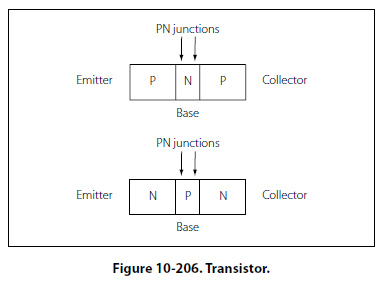
Diode Identification Figure 10-204 illustrates a number of methods employed for identifying diodes. Typically manufacturers place some form of an identifier on the diode to indicate which end is the anode and which end is the cathode. Dots, bands, colored bands, the letter ‘k’ or unusual shapes indicate the cathode end of the diode. Introduction to Transistors The transistor is a three-terminal device primarily used to amplify signals and control current within a circuit. [Figure 10-206] The basic two-junction semiconductor must have one type of region sandwiched between two of the other type. The three regions in a transistor are the collector (C), which is moderately doped, the emitter (E), which is heavily doped and the base (B) significantly less in its doping. The alternating layers of semiconductor material type provide the common commercial name for each type of transistor. The interface between the layers is called a junction. Selenium and germanium diodes previously discussed are examples of junction diodes. Note that the sandwiched layer or base is significantly thinner than the collector or the emitter. In general this permits a “punching through" action for the carriers passing between the collector and emitter terminals.
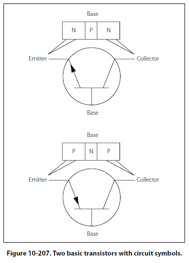
Classification The transistors are classified as either NPN or PNP according to the arrangement of their N and P-materials. The NPN transistor is formed by introducing a thin region of P-material between two regions of N-type material. The opposite is true for the PNP configuration. The two basic types of transistors along with their circuit symbols are shown in Figure 10-207. Note that the two symbols are different. The horizontal line
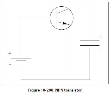
represents the base, and two angular lines represent the emitter and collector. The angular line with the arrow on it is the emitter, while the line without is the collector. The direction of the arrow on the emitter determines whether or not the transistor is a PNP or an NPN type. If the arrow is pointing in, the transistor is a PNP. On the other hand, if the arrow is pointing out, then it is an NPN type. Transistor Theory As discussed in the section on diodes, the movement of the electrons and holes can be considered current. Electron current moves in one direction, while hole current travels in the opposite direction. In transistors, both electrons and holes act as carriers of current. A forward biased PN junction is comparable to a low-resistance circuit element because it passes a high current for a given voltage. On the other hand, a reverse-biased PN junction is comparable to a highresistance circuit element. By using Ohm’s law formula for power (P = I2R) and assuming current is held constant through both junctions, it can be concluded that the power developed across the high resistance junction is greater than that developed across a low resistance junction. Therefore, if a crystal were to contain two PN junctions, one forward biased and the other reverse biased, and a low-power signal injected into the forward biased junction, a high power signal could be produced at the reverse-biased junction. To use the transistor as an amplifier, some sort of external bias voltage must modify each of the junctions. The first PN junction (emitter-base) is biased in the forward direction. This produces a low resistance. The second junction, which is the collector-base junction, is reverse biased to produce a high resistance. Figure 10-208 illustrates the proper biasing of an NPN transistor.
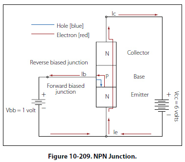
With the emitter-base junction biased in the forward direction, electrons leave the negative terminal of the battery and enter the N-material. These electrons pass easily through the emitter, cross over the junction, and combine with the hole in the P-material in the base. For each electron that fills a hole in the P-material, another electron will leave the P-material, which creates a new hole and enters the positive terminal of the battery. The second PN junction, which is the base-collector junction, is reverse biased. This will prevent the majority carriers from crossing the junction, thus creating a high resistance circuit. It is worth noting that there still is a small current passing through the reversed PN junction in the form of minority carriers — that is, electrons in the P-material and holes in the N-material. The minority carriers play a significant part in the operation of the NPN transistor. Figure 10-209 illustrates the basic interaction of the NPN junction. There are two batteries in the circuit used to bias the NPN transistor. Vbb is considered the base voltage supply, rated in this illustration at 1 volt, and the battery voltage Vcc, rated at 6 volts, is called the collector voltage supply.
Current within the external circuit is simply the movement of free electrons originating at the negative terminal of the battery and flowing to the N-material. This is shown in Figure 10-209 as Ie or emitter-current. As the electrons enter the N-material, they become the majority carrier and move through the N-material to the emitter-base PN junction. This emitter-base junction is forward biased at about 0.65 to 0.7 volts positive with respect to the emitter and presents no resistance to the flow of electrons from the emitter into the base, which is composed of P-material. As these electrons move into the base, they will drop into available holes. For every electron that drops into a hole, another electron exits the base by way of the base lead and becomes the base current or Ib. Of course, when one electron leaves the base, a new hole is formed. From the standpoint of the collector, these electrons that drop into holes are lost and of no use. To reduce this loss of electrons, the transistor is designed so that the base is very thin in relation to the emitter and collector, and the base is lightly doped. Most of the electrons that move into the base will fall under the influence of the reverse bias of the collector. While collector-base junction is reverse biased with respect to the majority carriers, it behaves as if it is forward biased to the electrons or minority carriers in this case. The electrons are accelerated through the collector-base junction and into the collector. The collector is comprised of the N-type material; therefore, the electrons once again become the majority carrier. Moving easily through the collector, the electrons return to the positive terminal of the collector supply battery Vcc, which is shown in Figure 10-209 as Ic. Because of the way this device operates to transfer current (and its internal resistances) from the original conduction path to another, its name is a combination of the words “transfer" and “resistor" — transistor. |
| ©AvStop Online Magazine Contact Us Return To Books |