![]()
|
|
||
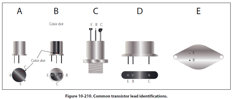
PNP Transistor Operation The PNP transistor generally works the same way as the NPN transistor. The primary difference is that the emitter, base, and collector materials are made of different material that the NPN. The majority and minority current carriers are the opposite in the PNP to that of the NPN. In the case of the PNP, the majority carriers are the holes instead of the electrons in the NPN transistor. To properly bias the PNP, the polarity of the bias network must be reversed. Identification of Transistors Figure 10-210 illustrates some of the more common transistor lead identifications. The methods of identifying leads will vary due to a lack of a standard and will require verification using manufacturer information to properly identify. However, a short description of the common methods is discussed below.
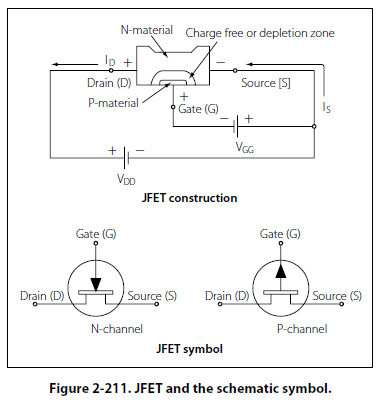
Illustration D in Figure 10-210 shows an oval-shaped transistor. The collector lead in this case is identified by the wide space between it and the lead for the base. The final lead at the far left is the emitter. In many cases, colored dots indicate the collector lead, and short leads relative to the other leads indicate the emitter. In a conventional power diode as seen in illustration E of Figure 10-210, the collector lead is usually a part of the mounting bases, while the emitter and collector are leads or tines protruding from the mounting surface. Field Effect Transistors Another transistor design that has become more important than the bipolar transistor is the field-effect transistor or FET. The primary difference between the bipolar transistor and the FET is that the bipolar transistor has two PN junctions and is a current controlled device, while the FET has only one PN junction and is a voltage controlled device. Within the FET family, there are two general categories of components. One category is called the junction FET (JFET), which has only one PN junction. The other category is known as the enhancement- type or metal-oxide JET (MOSFET). Figure 10-211 shows the basic construction of the JFET and the schematic symbol.
In this Figure, it can be seen that the drain (D) and source (S) are connected to an N-type material, and the gate (G) is connected to the P-type material. With gate voltage Vgg set to 0 volts and drain voltage Vdd set to some positive voltage, a current will flow between the source and the drain, through a narrow band of N-material. If then, Vgg is adjusted to some negative voltage, the PN junction will be reverse biased, and a depletion zone (no charge carriers) will be established at the PN junction. By reducing the region of noncarriers, it will have the effect of reducing the dimensions of the N-channel, resulting in a reduction of source to drain current. Because JFETs are voltage-controlled devices, they have some advantages over the bipolar transistor. One such advantage is that because the gate is reverse biased, the circuit that it is connected to sees the gate as a very high resistance. This means that the JFET has less of an insertion influence in the circuit. The high resistance also means that less current will be used. Like many other solid-state devices, careless handling and static electricity can damage the JFET. Technicians should take all precautions to prevent such damage. |
| ©AvStop Online Magazine Contact Us Return To Books |