![]()
|
|
||
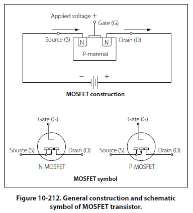
Metal-Oxide-Semiconductor FET (MOSFET) Figure 10-212 illustrates the general construction and the schematic symbol of the MOSFET transistor. The biasing arrangement for the MOSFET is essentially the same as that for the JFET. The term “enhancement" comes from the idea that when there is no bias voltage
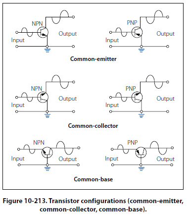
applied to the gate (G), then there is no channel for current conduction between the source (S) and the drain (D). By applying a greater voltage on the gate (G), the P-channel will begin to materialize and grow in size. Once this occurs, the source (S) to drain (D) current Id will increase. The schematic symbol reflects this characteristic by using a broken line to indicate that the channel does not exist without a gate bias. Common Transistor Configurations A transistor may be connected in one of three different configurations. The three basic configurations are: common-emitter (CE), common-base (CB), and common- collector (CC). The term “common" is used to indicate which element of the transistor is common to both the input and the output. Each configuration has its own characteristics, which makes each configuration suitable for particular applications. A way to determine what configuration you may find in a circuit is to first determine which of the three transistor elements is used for the input signal. Then, determine the element used for the output signal. At that point, the remaining element, (base, emitter, or collector) will be the common element to both the input and output, and thus you determine the configuration. Common-Emitter Configuration This is the configuration most commonly used in amplifier circuits because they provide good gains for voltage, current, and power. The input signal is applied to the base-emitter junction, which is forward biased (low resistance), and the output signal is taken off the collector-emitter junction, which is reverse biased (high resistance). Then the emitter is the common element to both input and output circuits. [Figure 10-213]
When the transistor is connected in a common-emitter configuration, the input signal is injected between the base and emitter, which is a low resistance, low-current circuit. As the input signal goes positive, it causes the base to go positive relative to the emitter. This causes a decrease in the forward bias, which in turn reduces the collector current IC and increases the collector voltage (EC being more negative). During the negative portion of the input signal, the voltage on the base is driven more negative relative to the emitter. This increases the forward bias and allows an increase in collector current IC and a decrease in collector voltage (EC being less negative and going positive). The collector current, which flows through the reverse-biased junction, also flows through a high resistance load resulting in a high level of amplification. Because the input signal to the common-emitter goes positive when the output goes negative, the two signals are 180° out of phase. This is the only configuration that provides a phase reversal. The common-emitter is the most popular of the three configurations because it has the best combination of current and voltage gain. Gain is a term used to indicate the magnitude of amplification. Each transistor configuration has its unique gain characteristics even though the same transistors are used. |
| ©AvStop Online Magazine Contact Us Return To Books |