TRANSISTORS
TRANSISTORS
| The transistor is an electronic device that is capable
of performing most of the functions of vacuum tubes. It is very small,
light in weight, and requires no heater. It is also mechanically rugged
and does not pick up stray signals. Transistors have been in general use
for more than a decade, but compared to some of the components they are
replacing they are relatively new. As research progresses, new discoveries
often cause some elements of transistor theory to be modified.
A transistor is a semiconductor device consisting of two types of materials
each of which exhibits electrical properties. Semiconductors are materials
whose resistive characteristics fall approximately midway between those
of good conductors and insulators. The interface between the parts is called
a junction. Selenium and germanium diodes (rectifiers) are examples of
such devices and are called junction diodes. Most transistors are made
of germanium to which certain impurities are added to impart certain characteristics.
The impurities used are generally arsenic or indium.
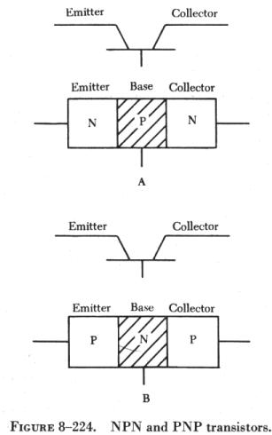
The type of transistor which may be used in some applications in place
of the triode tube is the "junction" transistor, which actually has two
junctions. It has an emitter, base, and collector which correspond to the
cathode, grid, and plate, respectively, in the triode tube. Junction transistors
are of two types, the NPN type and the PNP type (see figure 8-224). |
|
Theory of Transistor Operation
Before transistor operation and the meaning of "N" and "P" can be explained,
it is necessary to consider the theory of transistor action.
An electron is a negatively charged particle. In any material, there
are electrons separated from each other by some minute distance. Whenever
there is an electron, there is a negative charge. An atom of the semiconductor
material has a specified number of electrons, depending on the type of
material. If one of the electrons is removed, the hole from which the electrons
moved is more positive than the electron that was removed.
 |
The hole is considered to have a positive charge. If an electron from
a neighboring atom moves into the hole, the hole apparently moves to the
place from which the electron came. The hole does not really move; it is
filled in one place and formed in another. In A of figure 8-225, the electrons
are represented as black dots and the holes as dotted circles.
In B of figure 8-225, the electrons have moved one space to the left
of their position occupied in A of figure 8-225. In effect, the holes have,
therefore, moved one space to the right. |
The movement of the electrons is current. In the same sense, the movement
of holes is current also. Electron current moves in one direction; hole
current travels in the opposite direction. The movement of the charge is
a current. In transistors both electrons and holes act as carriers of current.
In transistors, materials referred to as N-materials and P-materials
are used. The N-materials are rich in electrons and, therefore, electrons
act as the carriers. The P-material is lacking in electrons and, therefore,
has holes as carriers.
An NPN transistor is not interchangeable with a PNP transistor and vice
versa. However, if all power supplies are reversed, they may be interchanged.
| Since temperature is critical in a transistor circuit,
there must be sufficient cooling for the transistors. Another precaution
to observe which applies to any circuit is: Power should never knowingly
be applied to an open circuit.
Diodes
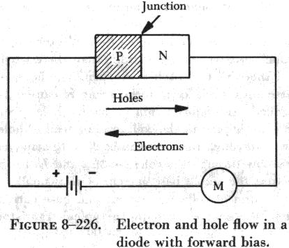
Figure 8-226 illustrates a germanium diode and consists of two different
types of semiconductor materials. With the battery connected as shown,
positive holes and electrons are repelled by the battery toward the junction,
causing an interaction between the holes and electrons. This results in
electrons flowing through the junction to the holes and to the positive
terminal of the battery. The holes move toward the negative terminal of
the battery. This is called the forward direction and is a "high" current. |
|
Connecting the battery as shown in figure 8-227 causes the holes and
electrons to be pulled away from the junction, and little interaction between
holes and electrons occurs at the junction. This results in very little
current flow, called reverse current.
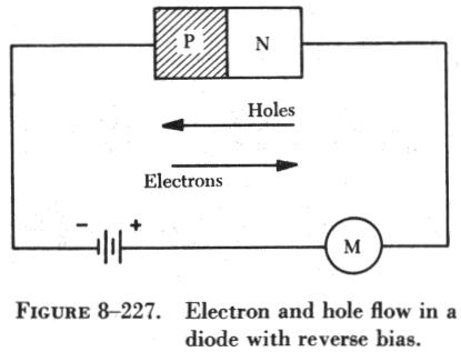
The potential on the electrodes of the transistor diodes applied from
the battery is called bias. It may be either forward or reverse bias, that
is, in a high current or a low current direction.
The N-germanium is manufactured with an impurity, such as arsenic, added
to give it an excess of electrons. Arsenic gives up its electrons readily
and can be used as a carrier. The P-germanium has an impurity, such as
indium, added. This takes the electrons from the germanium and leaves holes,
or positive carriers.
Zener Diodes
Zener diodes (sometimes called "breakdown diodes") are used primarily
for voltage regulation. They are designed so that they will break down
(allow current to pass) when the circuit potential is equal to or in excess
of the desired voltage. Below the desired voltage the zener blocks the
circuit like any other diode biased in the reverse direction. Because the
zener diode allows free flow in one direction when it is used in an ac
circuit, two diodes connected in opposite directions must be used. This
takes care of both alternations of current.
The zener may be used in many places where a gas filled vacuum tube
cannot be used, because it is smaller in size and can be used in low voltage
circuits. The gas filled tube is used in circuits above 75 volts, but the
zener diode may be used in regulating voltages as low as 3.5 volts.
PNP Transistor
Figure 8-228 shows a transistor circuit powered
by batteries. The emitter circuit is biased by the battery Ee in the forward
or high current flow direction. The collector circuit is biased by battery
E, in the reverse or low current flow direction. If the switch in the emitter
circuit were closed (collector switch open), a high emitter current would
flow since it is biased in the forward direction. If the collector switch
were closed (emitter switch open), a low current would flow since it is
biased in the reverse direction.
At the same time, a hole current is flowing in the opposite direction
in the same circuit, as shown in figure 8-229.
Hole current flows from the positive terminal of the battery, whereas electron
current originates at the negative terminal. The operation with both switches
closed is the same as with a PNP transistor, except that the emitter now
ejects electrons instead of holes into the base, and the collector, being
positive, will collect the electrons. There is again a large increase in
collector current with the emitter switch closed. With the emitter switch
open, the collector current will be small, since it is biased for reverse
flow.
At first glance it may appear that the transistor cannot amplify, since
there is less current in the collector than in the emitter circuit. Remember,
however, that the emitter is biased in the forward direction and a small
voltage causes a large current, which is equivalent to a low resistance.
The collector circuit is biased in the reverse direction, and a large voltage
causes a small current, which is the equivalent of a high resistance.
When both switches are closed, a phenomenon known as transistor action
occurs. The emitter, biased in the forward direction, has its positive
holes ejected through the junction into the "N" region of the base. (The
positive battery terminal repels the holes through the junction.) The collector,
being biased negatively, will now attract these holes through the junction
from the base to the collector.
This collecting of holes by the collector causes a much greater reverse
current than there would be if the emitter switch were open. The large
increase of reverse collector current is caused by so called transistor
action, whereby holes from the emitter pass to the collector. Instead of
holes flowing through the base and back to the emitter, they flow through
the collector, Ec, and Ee to the emitter; the actual base current is very
small.
The sum of collector current and base current equals the emitter current.
In typical transistors the collector current can be 80 - 99 percent of
the emitter current, with the remainder flowing through the base.
NPN Transistor
In figure 8-230 an NPN transistor is connected
into a circuit. Notice that the battery polarities are reversed from those
for the PNP transistor. But with the types of transistor material reversed,
the emitter is still biased in the forward direction, and the collector
is still biased in the reverse direction.
In this circuit a small signal applied to the input terminal causes
a small change in both emitter and collector currents; however, the collector,
being a high resistance, requires only a small current change to produce
large voltage changes. Therefore, an amplified signal appears at the output
terminals.
The circuit in this illustration is called a grounded base amplifier,
because the base is common to input and output (emitter and collector)
circuits.
Figure 8-231 shows a different type of circuit
connection. This is called a grounded emitter amplifier, and is similar
to a conventional triode amplifier. The emitter is like a cathode, the
base like a grid, and the collector like a plate. The collector is biased
for a reverse current flow.
If the input signal swings positive, as shown in Figure
8-231, it will aid the bias and increase base and emitter current.
This increases collector current, making the upper output terminal more
negative. On the next half cycle, the signal will oppose the bias and decrease
emitter and collector current. Therefore, the output will swing positive.
It is 180° out of phase with the input just as in the conventional
triode tube amplifier.
Since the base current is a very small part of the total emitter current,
it requires only a very small change in base current to cause a large change
in collector current. Therefore, it again amplifies the signal. This circuit
has the highest gain (output/input) of the various transistor amplifiers.
A PNP transistor could also be used if battery polarities were reversed.
Use of Transistors
Transistors can be used in all applications where vacuum tubes are used,
within certain limitations imposed by their physical characteristics. The
main disadvantage of transistors is their low power output and limited
frequency range. However, since they are approximately one one-thousandth
the physical size of a vacuum tube, they can be used in compact equipment.
Their weight, approximately one one-hundredth that of a vacuum tube, makes
the equipment much lighter. Their life is approximately three times that
of a vacuum tube, and their power requirement is only about one-tenth that
of a vacuum tube.
Transistors can be permanently damaged by heat or by reversed polarity
of the power supply. For this reason, care must be exercised when installing
them in a circuit to prevent these conditions.
Transistors can be installed in miniature tube sockets, or they can
be soldered directly into the circuits. There is no maintenance to be performed
on them other than to remove and replace them as necessary.
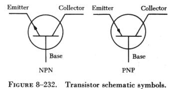
| When first tracing transistor circuits, trouble may be
experienced in understanding from the schematic whether a transistor is
an NPN or a PNP. Refer to figure 8-232, which shows the schematic symbol
for two types of transistors. Notice an arrow in the emitter line. When
this arrow is pointing away from the base, it is an NPN; if the arrow is
pointing toward the base, it is a PNP transistor.
A simple rule to determine whether the transistor is a PNP or an NPN
is as follows: If it is a PNP, the center letter "N" indicates a negative
base or, in other words, that the base will conduct more freely on a negative
charge. If the transistor is an NPN, the "P" indicates a positive base
and the transistor will conduct more freely on a positive base charge. |
|
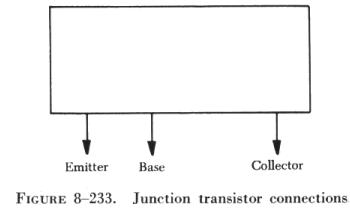 |
Since there are different types of transistors based on the method
used in their manufacture, there are several means of identifying the transistor
in a circuit as either an NPN or a PNP. One method used to identify the
type of transistor, called the junction transistor, is illustrated in figure
8-233. In this case, the method used to determine which of the three wires
connected to a transistor is the base lead, which is the collector lead,
and which is the emitter lead is based on the physical spacing of the leads.
Notice that there are two leads close together and one lead further apart.
The center lead is always the base. The lead closest to the base is the
emitter lead, and the lead further out is the collector lead. The schematic
shown in this illustration holds true for all junction-type transistors.
For detailed information on any transistor, the applicable manufacturer's
publications should be consulted. |